Semiconductor nanostructures
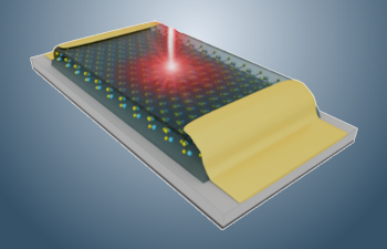
 Over the last two decades, artificial structures have become the cutting edge of semiconductor physics. These structures can be grown by a variety of methods, such as molecular beam epitaxy or metal-organic vapour deposition. They consist of semiconductor layers with interface geometry, doping level and chemical composition defined with atomic-scale precision. The characteristic features of the heterostructures are interfaces between different materials which restrict the motion of the electrons to two, one or zero dimensions. We have been working in transport properties of semiconductor superlattices driven by electric fields. As growth defects always appear in superlattices, we have developed some models to include interface roughness scattering. Recently we have been involved with time dependent phenomena in dc fields (Bloch oscillations) and in ac-dc fields (Rabi oscillations).